In the rush to cash in on the Internet-of-Things, manufacturers often rely on “security by obscurity” to protect their products. However, keeping the details of their implementations secret by locking the microcontroller interfaces so that no one can see—and tamper with—the firmware on the chips does not prevent attacks. It just prevents security researchers from finding design flaws and security vulnerabilities so that they can be fixed.
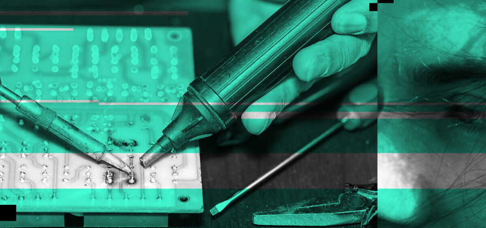
If security researchers are to help make these devices secure, then they need to be able to access the contents of the chips. They may look at the firmware to ensure the instructions don't contain a logic flaw. They may look at the protections on special data (such as keys) stored on the chip. One of the ways to get access to the contents is via an “invasive” class of attacks, which manipulates the silicon die without affecting chip functionality.
The process has been out of reach for most researchers, until now. Mikhail Davidov, a principal security researcher at Duo Labs has developed a technique that makes it possible for researchers to get past the barriers on the chip and access the microcontroller directly.
“Researchers don't need a multi-million dollar lab to perform practical invasive attacks against a typical microcontroller,” Mikhail Davidov, a principal security researcher at Duo Labs, wrote in an extensive write-up of his decapsulation technique.
When building their products, manufacturers program chips with instructions for the microcontroller to execute. The chip has configuration flags to prevent foreign processes from reading what was written. Once code is programmed into the microcontroller and marked as being protected, the only way to read the contents is to also destroy the programmed code.
The decapsulation process makes it possible to flip the configuration flags so that read-access is possible again while keeping the code intact on the chip. While Davidov focused his efforts on extracting “supposedly inaccessible code” stored on the microcontroller, this same process can be used for things like firmware recovery and optical glitching. Optical glitching refers to using a light source to manipulate internal circuits or switch individual transistors.
How the process works
Chips are made out of “painstakingly processed bits of silicon and tiny wires” and then covered by a hard epoxy, a specialized molding compound, which makes the whole thing more durable and prevent direct access to the wires. Etching is a chemical method for breaking down and washing away that hard layer without damaging the silicon or the wires.
“I'm removing that packages to get to the parts that do the actual work,” Davidov said. “It's like opening the cover of a book to see what is written inside.”
Davidov first removed the material manually—with a belt grinder to sand down the edges until he could see the edge of the silver-colored die. Once he could see the location of the bond wires, he switched to a more precise tool to remove the rest of the material. The goal was to repeatedly cut away the material and get as close to the bond wires as possible. “A 3D-printer with a Dremel strapped to the side” did the job.
The next step was etching, with a solution of nitric acid and sulfuric acid. Davidov provided detailed lab safety instructions, warning that the fumes released during etching can be dangerous. The most dangerous part was taking out the small quantities of the acids (2 mL to 3 mL at a time) from the larger bottles to prepare the etchant, Davidov said.
Etching itself was “gentle and slow,” waiting for the acid to react with the piece, rinsing in an acetone bath, and repeating the process until the bond wires were visible and the silicon die was fully exposed. How long the process would take depends on the type of chip—the height of the wires as well as how much of the epoxy material had already been removed.
“From start to finish, I can get it done in about six hours where the majority of my time is spent doing something else as I wait for the acid to do its work," Davidov said.
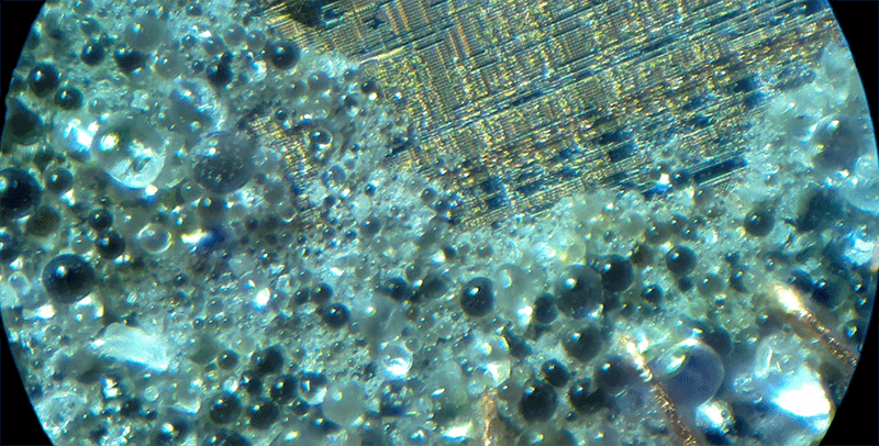
After putting the chemistry set away, Davidov used a microscope to look for the floating-gate transistor array—a relatively large uniform texture surrounded by row and column drivers—on the silicon die. Data is stored in flash memory by trapping little bits of charge inside the silicon. When the silicon is exposed to high-energy ultraviolet light, the trapped charge escapes, thus changing the value stored. This way, he could reset all the configuration flags on the chips.
Davidov found that for the microcontrollers he was working with, the configuration flags were stored in a separate section of the chip from where the rest of the program code was written. He covered up the section holding the program code with nail polish to protect that section from the UV light. If the configuration flags had been stored closer, or in the same location as the program code, it would have been “extremely difficult, if not impossible,” to apply the nail polish to protect the program code from being erased.

While Davidov was able to access the data on his microcontroller, this doesn't mean all hardware chips can be exposed with this process. More security-focused mircocontrollers like the ones used in hardware security modules (HSM) to store encryption keys, trusted platform modules (TPM), and SIM-cards have have hardened chipsets to make these invasive attacks more challenging, Davidov said. They have countermeasures such as protective shielding and an active mesh layer to detect when a trace has been cut. Light sensors, when tripped, could automatically destroy all stored secrets if the chip powered on after the molding component was removed.
While there are ways to bypass these features, they require extremely specialized equipment and “significant investment.”
Davidov found the security key (used for authentication) from Yubico, the YK4 Nano, had such countermeasures. When looked at under the microscope after etching, Davidov said “pretty much every active part of the die apart from the bond pads is shielded by a metal layer," preventing visual inspection and UV tampering. Trying to get past the layer would likely render the circuit non-functional, he said.
For non-security hardened microcontrollers, this technique is sufficient for accessing the silicon layer and would be useful for security researchers interested in expanding the scope of their work with hardware. More tools lead to more vulnerability discovery, which would result in better product security, eventually.